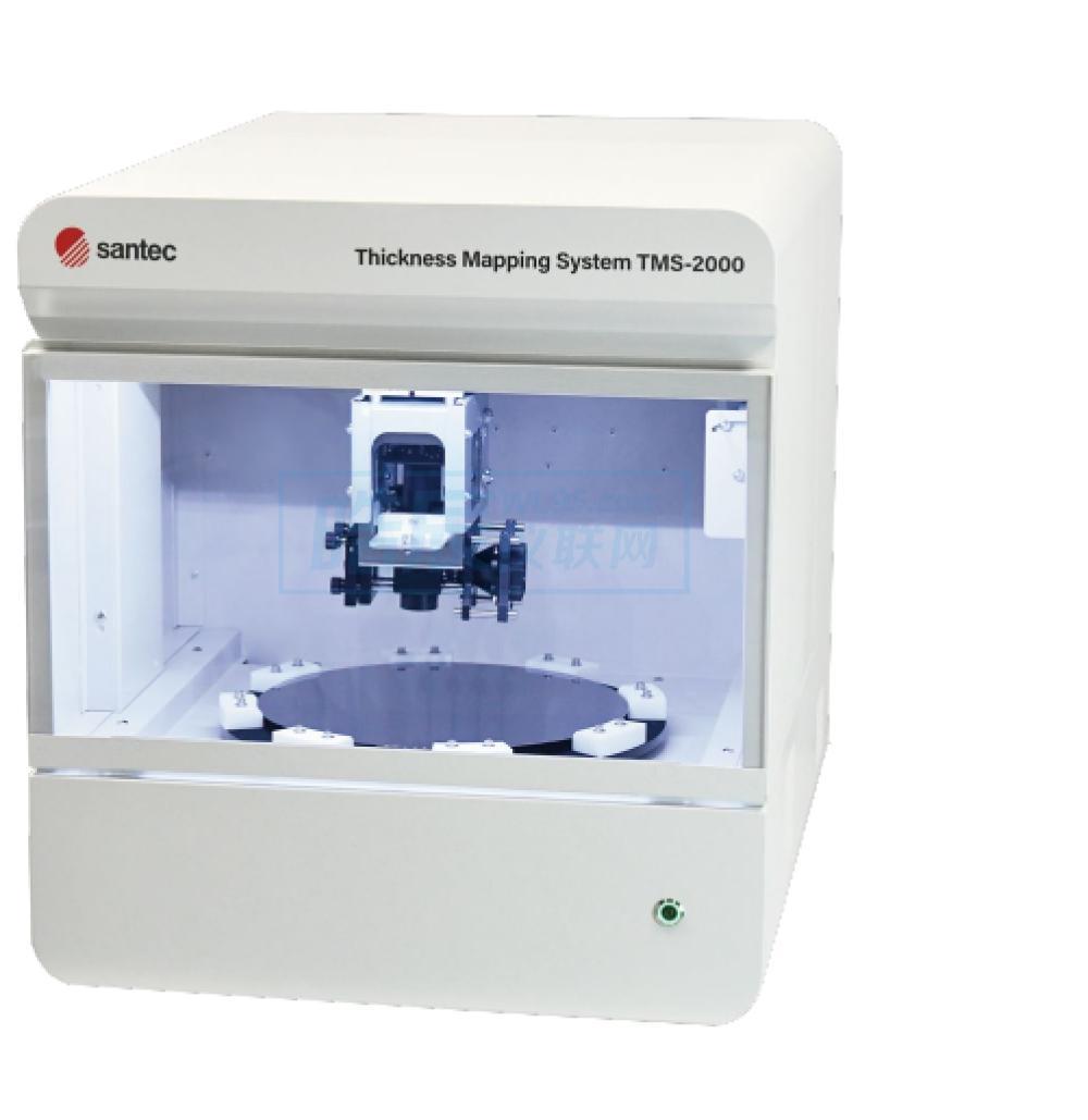
Product Overview:
The new system from Santec, the TMS-2000, brings a new dynamic to high accuracy sub-nanometer mapping of semiconductor wafer thickness. Utilizing a novel laser scanning method, not previously used in the industry for wafer mapping, the TMS-2000 offers several benefits to the industry; accurate thickness measurements that are insensitive to temperature variations, a single system to measure not just Si single layers but also power semiconductors such as SiC and GaN, as well as multi-layer wafers like SOI, at a cost point that is attractive for widespread deployment in production. As semiconductor devices reduce in size, the tolerances for the lithography processes become finer, raising the importance of high accuracy in wafer thickness and site flatness measurements. For non-contact, sub-nanometer repeatability measurements the industry has relied on heterodyne interference or Fizeau fringe analysis systems that have several drawbacks for universal adoption. These current solutions require front and back wafer illumination, are sensitive to temperature variations and vibrations, and are high in complexity and cost. The Santec TMS-2000 addresses all those concerns found with the present solutions.
Features:
High Accuracy:High accuracy measurement using interferometric detection technique (1nm repeatability)
Industry Standard Parameters:Analysis of Global (GFLR, GFLD, GBIR), Site (SFQR, SFQD, SBIR), Edge (ESFQR) possible
High Environmental Resistance:No temperature control or vibration countermeasures are required due to environmental durability
Compact Size:Small form factor suitable for multiple applications
High Speed:Spiral Scanning (High speed, high density)
Advantages:
Wafer thickness measurement system that can measure the flatness of the wafer up to 1nm repeatability.
Accurate measurements, insensitive to temperature variations and vibrations
Sub-nanometer thickness repeatability
Full wafer mapping with customizable scan patterns
Single side illumination
Wafer-to-wafer comparisons
Suitable for heavily doped Si as well as power semiconductors and multi-layer wafers
Measurements compliant with SEMI standards
Cost advantage over conventional solution


 服务热线:0755-86016691 电话:13715327187 传真:0755-86641139-816