
您好 欢迎来到晧辰科技!    [登录] [注册]
晧辰仪联网
新闻动态|全新仪器|资讯论坛
快捷发布|产品促销|资料中心

所有设备分类

新闻动态

促销信息

产品详情

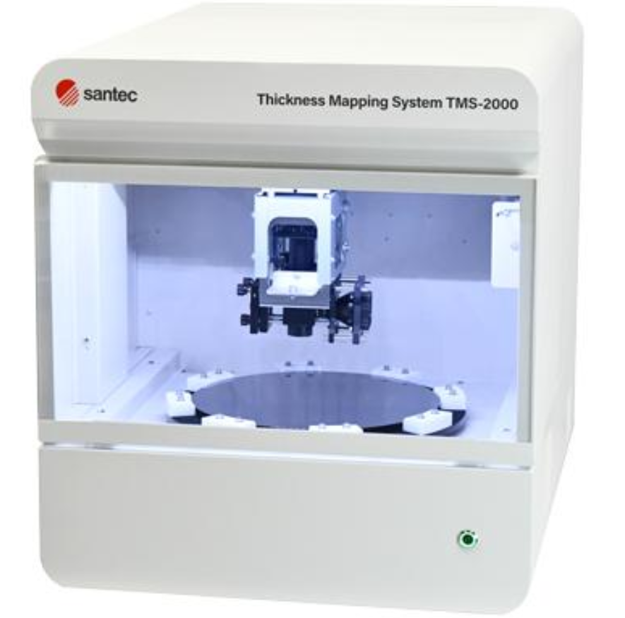
销售圣德科 TMS-2000 高重复性模型

浏览次数:4

晧辰自营,品质保证,配送快捷

产品参数

选件 是否计量 发货周期 保修时间 成色
否 7天 90天 全新
所在地 机身号 状态 资料下载
深圳市 完好
更新日期:2026-07-15
联系电话:0755-86016691

* 产品描述

产品描述:

Santec 的新系统 TMS-2000 为半导体晶圆厚度的高精度亚纳米测绘带来了新的动态。 TMS-2000 采用一种新颖的激光扫描方法(以前未在行业中用于晶圆测绘),为行业带来了多项优势;对温度变化不敏感的精确厚度测量,单个系统不仅可以测量 Si 单层,还可以测量 SiC 和 GaN 等功率半导体以及 SOI 等多层晶圆,其成本点对生产中广泛部署具有吸引力。随着半导体器件尺寸的减小,光刻工艺的公差变得更加精细,提高了晶圆厚度和场地平整度测量的高精度的重要性。对于非接触式,业界一直依赖外差干涉或斐索条纹分析系统进行亚纳米精度测量,但这些系统在普遍采用方面存在一些缺点。当前的这些解决方案需要正面和背面晶圆照明,对温度变化和振动敏感,并且复杂性和成本很高。 Santec TMS-2000 解决了当前解决方案中发现的所有问题。


产品特点:

精确测量对温度变化和振动不敏感

亚纳米厚度重复性

具有可定制扫描模式的完整晶圆映射

单面照明

晶圆间比较

适用于重掺杂硅以及功率半导体和多层晶圆

测量符合 SEMI 标准

相对于传统解决方案的成本优势
详细信息

Product Description:
 
Santec's new system TMS-2000 brings a new dynamic to high-precision subnanometer mapping of semiconductor wafer thickness. The TMS-2000 employs a novel laser scanning method (not previously used in the industry for wafer mapping) that brings several advantages to the industry; With accurate thickness measurements that are insensitive to temperature changes, a single system can measure not only Si monolayers but also power semiconductors such as SiC and GaN and multilayer wafers such as SOI at a cost point that is attractive for widespread deployment in production. As the size of semiconductor devices decreases, the tolerances of lithography processes become finer, increasing the importance of high accuracy in wafer thickness and field flatness measurements. For non-contact, the industry has been relying on heterodyne interference or Fizau fringe analysis systems for subnanometer accuracy measurements, but these systems have some drawbacks in terms of general adoption. These current solutions require front and back wafer lighting, are sensitive to temperature changes and vibration, and are complex and costly. Santec TMS-2000 addresses all the issues found in current solutions.
 
Product Features:
 
Accurate measurements are not sensitive to temperature changes and vibrations
Sub-nanometer thickness repeatability
Complete wafer mapping with customizable scan patterns
Single side lighting
Wafer to wafer comparison
Suitable for heavily doped silicon as well as power semiconductors and multilayer wafers
The measurement conforms to SEMI standard
Cost advantages over traditional solutions

同类热门仪器

友情推荐

合作客户:

查看更多>>

国产仪器:

查看更多>>

进口仪器:

查看更多>>

校准计量:

查看更多>>

联系我们

QQ

在线QQ服务

立即联系

服务热线

0755-86016691

13602653900

传真

0755-86641139-816

电子邮箱

info@wl95.com

Copyright © 2007 All Rights Reserved. 深圳市晧辰电子科技有限公司 版权所有  [粤ICP备14101712号-1] [法律顾问]

公司地址:广东省深圳市南山区南山智谷产业园F座1402  邮编:518055