Product Description:
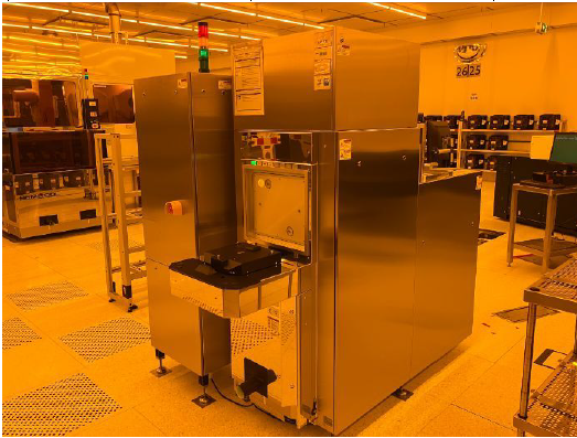
The HSEB MMT 300 Wafer Inspection microscope (perhaps also known as the MT-300 Semiconductor Inspection Microscope) is a high-precision inspection device specifically designed for the semiconductor industry. It is suitable for the observation and measurement of various electronic components, wafers and large samples, and can meet the demand for high-precision and high-sensitivity inspection equipment in the semiconductor manufacturing process.
Features:
Equipped with polarizing device (straight deviation, deviation detector).
Desktop computer with high configuration (such as 8GB memory, 500GB hard disk, DVD drive, keyboard and mouse, and 21.5-inch LCD display).
The measurement software has powerful functions, including two-dimensional geometric measurement functions (such as distance between two points, distance from point to line, Angle, center distance, etc.) and cross line display function.
The weight of the instrument is 320Kg and the structure is stable.