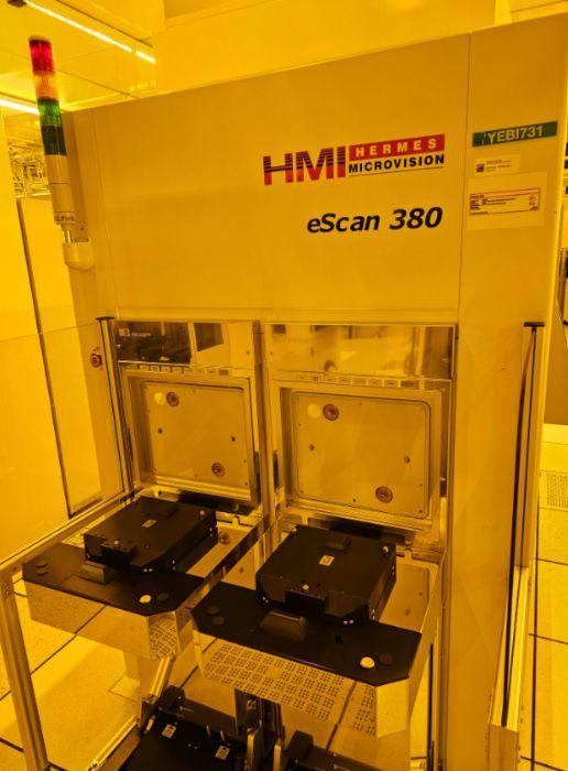
Product Description:
Scanning electron microscopy uses a focused high-energy electron beam to scan the surface of the sample, and through the interaction of the electron beam with the sample material, various physical signals (such as secondary electrons, backscattered electrons, etc.) are excited. These signals are collected, amplified, and converted into image information to achieve the characterization of the surface microstructure of the sample.
Features:
High resolution: The resolution of the new scanning electron microscope can reach 1nm, which can clearly observe the tiny details of the sample surface.
Large depth of field and stereo imaging: the depth of field is large, the field of view is large, and the imaging stereo effect is good, which helps to understand the three-dimensional structure of the sample more accurately.
Adjustable magnification: the magnification can reach 300,000 times and above, and it is continuously adjustable, and the appropriate magnification can be selected according to the need for observation.
Sample adaptability: Many types of samples can be analyzed, including conductive and non-conductive materials (conductive treatment required).
Versatility: In addition to observing the microscopic morphology of the sample, it can also be combined with other analytical instruments for microcomponent analysis of the substance.