Product Description:
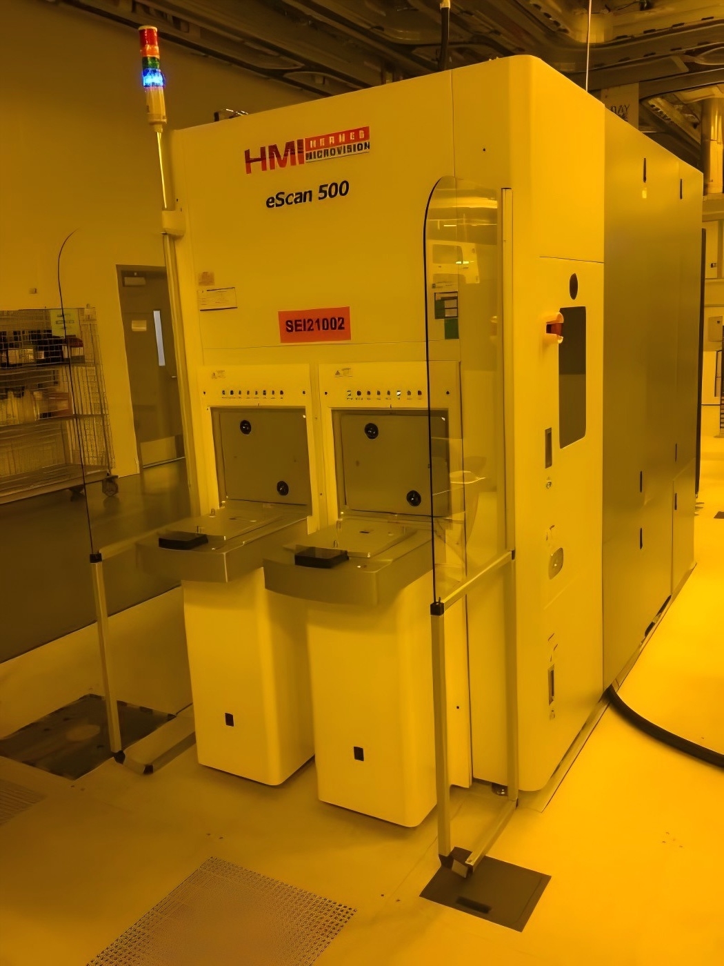
HERMES MICROVISION/HMI eScan 500 is a high-resolution mask and wafer inspection device that uses laser scanning to detect and measure defects on semiconductor materials. The HMI eScan 500 features a wide exposure range, large field of view and high sensitivity, all optimized to detect the smallest defects on semiconductor device surfaces. The HERMES MICROVISION eScan 500 is an advanced system consisting of a sophisticated optical microimaging setup, a fast scanning phase and an optically stabilized solid-state image detector. The optical device consists of a high-resolution telecentric optical element with an adjustable numerical aperture and fieldStop aperture. This arrangement ensures that the image is always sharply focused on the detector, regardless of the sample position. The rapid scan phase allows for a wide field of view, covering the entire sample with minimal repositioning and substrate alignment time. The detector is a 32-megapixel backlit CMOS sensor that captures high-sensitivity, large-field images through a variety of optical filters. The pace of eScan 500 acquisitions has been particularly impressive; Scan up to 1 million pixels per second. This allows it to examine every region of a given sample in a reliable and timely manner. The HERMES MICROVISION/HMI eScan 500 also provides programmable Settings for brightness, contrast, zoom, focus and scan resolution. This ensures that the most original images are produced so that defects can be accurately sized and analyzed each time. In addition to high performance, the HMI eScan 500 is also cost-effective. The machine's low cost ensures that it is an attractive option for small chip manufacturers who lack the budget to buy large, expensive systems. In addition, the tool has excellent ease of use and requires little maintenance. Overall, the HERMES MICROVISION eScan 500 is an excellent mask and wafer inspection asset at a good price. eScan 500 has a wide field of view, fast scanning speed, and powerful defect detection capabilities to reliably detect the smallest defects on semiconductor materials with minimal effort and cost.
Features:
It can be used for physical defect detection in backscattered electron (BSE) mode
Provides extremely high defect detection resolution to identify subdesign regular pattern defects
Includes many features to improve inspection throughput. Our patented technology enables a uniquely large field of view (120 μm x 120 μm) that increases flux in skip scan mode without compromising sensitivity.