Product Description:
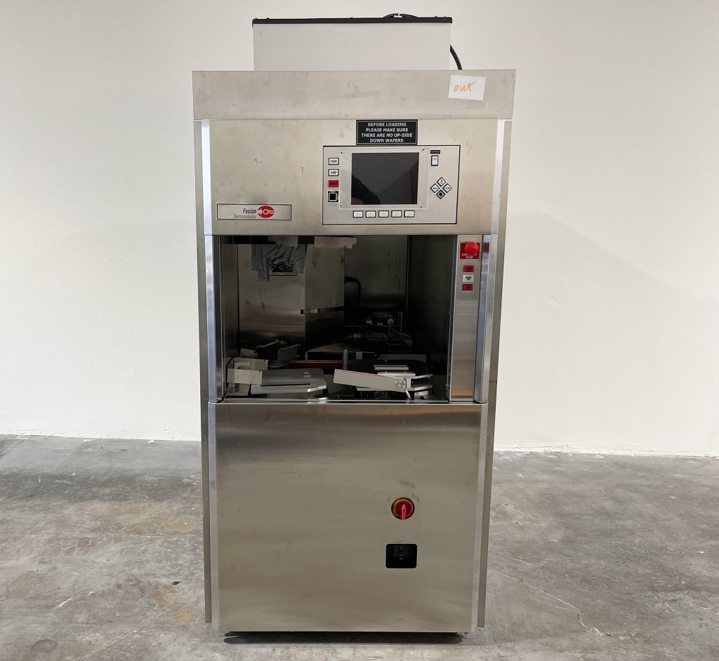
The AXCELIS/FUSION 200 ACU is an automatic exposure device designed to expose patterned silicon wafers to ultraviolet light. The system utilizes advanced technologies such as laser diarrhea arrays, pattern recognition optics, position sensors, and computer-controlled motion systems to precisely expose wafers to a variety of applications. The FUSION 200 ACU features a highly efficient laser diode array capable of emitting ultraviolet light at up to 1,000 watts of power, resulting in higher throughput than conventional exposure systems. The laser diode array is based on advanced optical technology and is self-calibrated, allowing for greater accuracy and repeated exposure patterns within a single chip. This unit can also be recessed into polygons, circles, ellipses, rectangles, and hexagons, as well as periodic and aperiodic patterns or grids. AXCELIS 'automatic pattern recognition and Precision Optics 200ACU allow for exposure area quality (EZQ) analysis on the chip, enabling accurate identification and precise exposure of pattern wafers in a single channel, and the machine also uses a built-in endpoint detection method to accurately detect when the wafers are fully exposed. In addition, the 200ACU uses an advanced motion system to precisely move the wafer between the laser diode array and the exposure run, precisely verifying the position of the pattern on the wafer with a position sensor. This ensures that the array is accurately exposed, regardless of array size, orientation, or complexity. This automated and precise exposure tool is capable of accommodating a variety of wafers, including 3 ", 5 ", 8 "and 12" wafers, and is user-friendly, providing users with a flexible way to fine-tune the asset to meet their specific process needs. With its robust and reliable design, the 200 ACU is an excellent choice for any production process involving array silicon wafers.