Product Description:
Feature reduction is a major factor in reducing semiconductor costs, and chip manufacturers continue to shrink their designs as aggressively as possible. Today, this shrinkage is achieved by single-exposure immersion lithography. Dual graphics technology using immersion scanners will also be used to shrink chip features and continue Moore's Law, which states that the number of transistors on a chip doubles every 24 months.
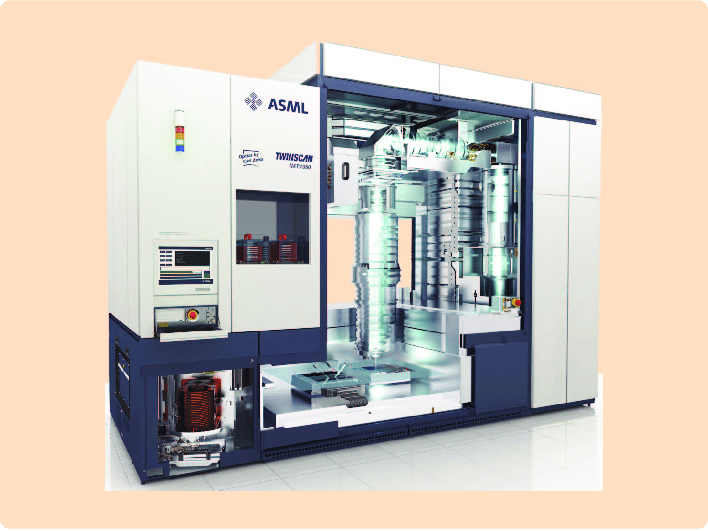
Dual graphics poses a productivity challenge for chipmakers because key layers of a chip need to be exposed and processed twice, which adds complexity and cost. At the same time, chipmakers need more efficient single graphics processes to stay competitive. ASML addresses these challenges with the new TWINSCAN NXT platform. As announced in October this year, the TWINSCAN NXT platform is based on the proven TWINSCAN dual-level architecture. New to the TWINSCAN NXT is an improved dual-platform design with higher acceleration, increased maximum scanning speed, and reduced overhead time through seamless platform exchange. As a result, the TWINSCAN NXT: 1950i is designed to produce more than 200 wafers per hour, which will allow chipmakers to process 30 percent more wafers per hour than today's most advanced systems. ASML expects TWINSCAN NXT: 1950i to process more than 4,000 wafers per day in mass production of memory chips.