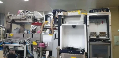
Product Description:
The ASML AT-850C is an advanced chip stepper designed to accurately and precisely define the microscopic mode of the latest generation of semiconductor wafers in the semiconductor industry. By projecting light onto thin layers of photoresist deposited on a wafer, it is possible to create precise patterns that form the basis of silicate components used in integrated circuits. The ASML AT850C is a fully automated scanner that scans the entire wafer sheet in a single rotation, allowing images to be projected onto the entire surface area of the wafer at once. This allows for efficient and consistent lithography. With a stage size of 350 mm, the system allows multiple different chips to be placed on the stage at once, enabling multiple processing runs. The AT:850C has been designed for advanced functionality with higher throughput instances. This includes an integrated, robust Litho Inspector that monitors drawings, defects, and other lithographic issues during production runs. The chip stepper has advanced stages that provide superior alignment control for even the smallest features. These stages can also execute processes at two different rotation speeds, giving users greater control over multiple processes. The ASML AT 850C also employs a variety of lighting methods, including laser direct imaging (LDI) and lithography imaging (PI). Using either of these imaging methods, high-resolution images can be created by exposing different areas of the wafer to different levels of light radiation. Properties as small as 0.35 microns can be resolved, allowing the AT850 C to produce highly intricate and delicate silicon components. The ASML AT 850 C also features advanced synchronous and asynchronous motion control and dynamics for extremely fast scan speeds and repeatability. The system is based on a modular platform, which means it can be customized for specific applications and processes, giving users complete flexibility. Finally, the AT850C is an extremely robust, robust, and reliable stepper that is constantly subjected to rigorous quality assurance testing to ensure that it is always operating at peak performance. With its advanced features and production capabilities, it is one of the most technologically advanced wafer steppers on the market today.