Product Description:
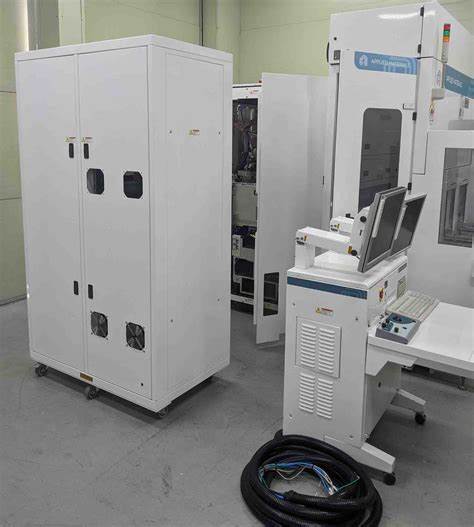
SEMVision G3 Lite is part of Applied Materials' SEMVision G3 family, the industry's fastest and most sensitive line of defect review and analysis tools for manufacturing at 65/45nm and above. The three systems in the new line set an industry benchmark with a sensitivity of 30 nanometers and throughput of up to 1,800 defects per hour. AMAT/APPLIED MATERIALS SemVision G3 Lite is a mask and wafer inspection device that provides automated, high-resolution inspection of photomasks, microelectronics and displays. The system is ideal for analyzing critical defects that are difficult to detect with standard optical inspection systems. The device uses an automated high-resolution imager with a 10x rotating motion stage that can be viewed in the 600mm x 600mm range. The tool also features a high-speed digital signal processor to quickly inspect multiple parts in a short amount of time. The optical element uses an optical microscope and an adjustable focusing base. The adjustable base allows depth of field adjustment and is equipped with a motorized co-step mechanism for precise stage movement. The asset's image processing software suite provides highly reliable and accurate detection of defects such as particle contamination, scratches, pinholes, film thickness changes, and other types of defects. The software also incorporates image analysis techniques such as pattern recognition, clustering and dimensional measurement. The software is integrated with the Triad MEA platform for rapid image capture and analysis. The model also includes a mouse interface that controls stage motion, zooming, and focusing. Operators also have access to web-based remote applications to manage equipment, monitor real-time performance, update parameters, and view and export captured images. The system's advanced measurement, accuracy, and performance capabilities make it ideal for use in semiconductor, FPD, and photomask production environments. In addition, the device can be used for the development of new processes and materials as well as quality control, wafer inspection and dielectric layer inspection.