Product Description:
CVD technology is crucial in semiconductor processing, whether logic devices, DRAM, NAND, or MEMS, optoelectronic devices, iot and power devices in the MtM market segment, CVD is an indispensable device for all semiconductor device manufacturing. Applied's Producer platform has become the foundation for the development of a variety of films, each with its own unique set of process requirements, and deposited on the same shape of a variety of geometric structures (blanket, gap filling, conformal), the Producer platform can be well suited to meet these technical needs.
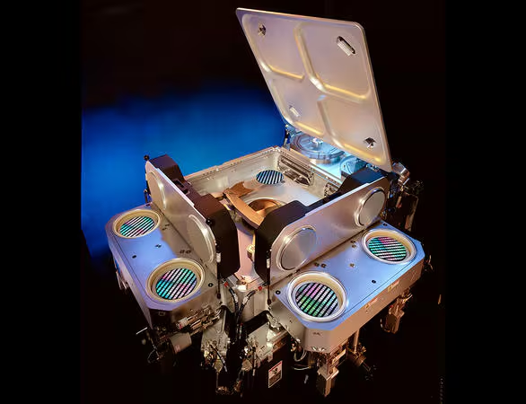
The Producer platform, which can handle 150mm, 200mm and 300mm wafers, has crossed a key technical inflection point (10 nodes) since its introduction in 1998, making it one of the most successful platforms ever. Its innovative Twin Chamber™ dual-chamber structure can process up to six wafers simultaneously for excellent production efficiency. With ceramic heaters and chamber components, as well as a remote plasma source for chamber cleaning, the Producer system minimizes the defect rate of CVD films. From loading cavity wafer mapping, to clear wafer orientation, to wafer placement, the platform reliably and meticulously handles a variety of MtM substrates, including silicon carbide wafers.
In addition to traditional PECVD (TEOS and silane-based oxides and nitrous compounds) and subatmospheric pressure CVD films, Producer systems are also suitable for low dielectric constant, strain engineering, photoetching films as well as hot films, high temperature PECVD applications, silicon germanium (SiGe) and amorphous silicon (a-Si). Some examples of its applications in MtM devices include thicker films (≥20µm), lower temperature processes (180°-350°C), more conformal films, and new materials such as low-temperature PECVD silicon-germanium (<50um) and amorphous silicon (a-Si).
The extensibility of the platform allows customers to use Producer tool components for multiple device types and process nodes.