Product description
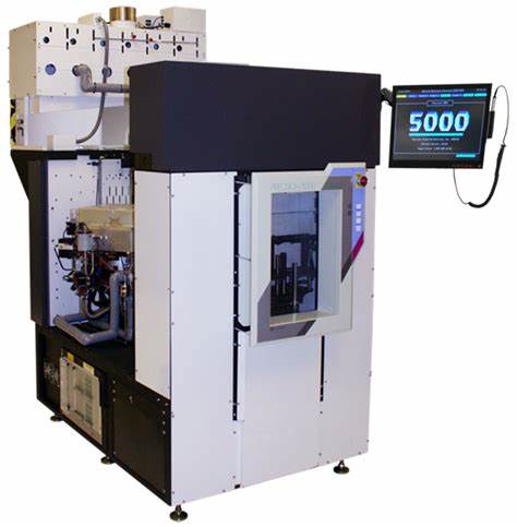
The Applied Materials P5000 is a plasma-enhanced chemical vapor deposition (PECVD) system designed to deposit thin film dielectrics and doped and undoped silicon, which contains semiconductor films deposited by a gas source that react in a plasma to form conformal and uniform films. The tool can be used to deposit silicon nitride (SiN), amorphous silicon (a_Si), phosphorus-doped silicon and boron-doped silicon films. Nitrous oxide (N2O) gas is available, so silicon dioxide (SiO2) can also be deposited.
Plasma-enhanced chemical vapor deposition is a chemical deposition technique that uses a reactive gas source and plasma to produce a conformal thin dielectric or semiconductor film at a certain temperature (up to 400°C for PECVD and up to 800°C for pyrolytic chemical vapor deposition). Before introducing the substrate from the vacuum load lock to the vacuum chamber, the vacuum chamber should be vacuumed to less than 50mtorr (6.67 kPa) to reduce atmospheric contaminants. A series of lifting pins on the chamber receptors can be lifted and lowered, allowing the robot to safely place the substrate. Then, before introducing any process gas, adjust the commutator spacing to within 1 mil (25.4 microns) of the required commutator/cap spacing.
Process gases are controlled by a series of pneumatic safety valves, and a single mass flow controller (MFC) regulates the mass flow of each individual process gas. Process gases are introduced into a temperature-controlled process chamber where the substrate is at rest. Butterfly valves, swing valves or other throttling devices are used to separately control the internal pressure without regulating the gas flow.
Once all process parameters (gas flow, chamber pressure, temperature, and receptor spacing) are stabilized, the radio frequency (RF) generator is activated. The most common frequency associated with PECVD is the industrially available 13.56 MHz frequency, although higher and lower frequencies have been used. The RF signal is modulated and tuned to a matching impedance of 50 ohms by means of a series of variable and fixed capacitors and inductors set in the L-matching circuit.
Although the plasma is generated by an AC source, there is DC self-bias due to blocking capacitors in the matching network. As a result, a build-up of electrons may occur on the energized electrode. This DC self-bias results in the directivity (i.e., anisotropy) of reactive ion etching and helps to improve the consistency of PECVD films through ion bombardment planarization. However, most PECVD chambers do not place the substrate on the energized electrode due to the increased membrane stress that can result from ion bombardment.
Plasma is a gaseous state of matter that contains ions, free radicals and molecules. It is usually formed when a gas is ionized. The main reactants in the film deposition process are highly active free radicals and ions formed in the plasma. The reactants are adsorbed to the surface, where they react and create a solid film. The by-product gas is desorbed and pumped out of the reaction chamber along with any unused reactants.