Product Description:
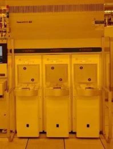
NanoSEM 3D critical size Scanning electron microscopy combines the high-resolution imaging capabilities of scanning electron microscopy (SEM) with the high-precision requirements of critical size (CD) measurements and is specifically designed for critical size measurements in semiconductor manufacturing processes. It provides measurement accuracy at the nanoscale, ensuring the performance and reliability of semiconductor devices.
Features:
High-resolution imaging: NanoSEM 3D has high-resolution imaging capabilities to clearly display the microstructure and morphology of the wafer surface. This helps to accurately measure and analyze the fine pattern sizes of semiconductor devices.
High precision measurement: The equipment uses advanced measurement technology and algorithms to achieve high precision and high repeatability of dimensional measurement. This is essential for quality control and process optimization in semiconductor manufacturing.
3D measurement capability: NanoSEM 3D not only has 2D dimension measurement capability, but also can perform 3D topography measurement and analysis. This contributes to a more complete understanding of the structure and performance of semiconductor devices.
Automated measurement: The equipment is equipped with an automated measurement system that automatically identifies and measures the target pattern on the wafer, improving measurement efficiency and accuracy.
User friendly interface: NanoSEM 3D's operating interface is simple and clear, easy to use and operate. At the same time, the device also provides rich data processing and analysis functions, which is convenient for users to carry out subsequent data processing and analysis.