Product Description:
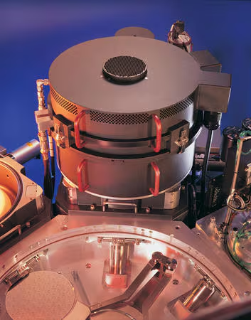
Applied Materials' Centura etching systems offer high productivity silicon, metal and dielectric etching. Etching is one of the most critical but challenging operations in semiconductor production operations. Whether it's etched gates, transistor isolation grooves, high aspect ratio contacts, or any level of interconnecting metal or dielectric film, maintaining accurate, repeatable, and uniform control of critical dimensions is key to device yield. Designed for 150mm and 200mm wafer sizes, the system addresses technical challenges, including high aspect ratio etchings for a range of MtM applications (<110: 1), including integrated hard mask trenching strips for shallow junction MOSFETs, and new materials such as indium tin oxide, silicon carbide (SiC), InGaAlP, GaAs, and gallium nitride for power devices and leds.
Centura and Centura AP host single-wafer, multi-chamber architectures enable integrated sequential wafer processing of 150 mm, 200 mm, and 300 mm wafers in up to four process chambers.
For 150/200mm wafers, the Applied Materials Centura DPS DTM system uses advanced deep reactive ion etching (DRIE) on a range of materials to precisely control the smoothness of the etched wall and the groove profile, while providing high aspect ratio capability and achieving high throughput. Applied Materials Centura DPS Plus is the industry standard for metal etching processes.
For 200/300 mm wafers, Applied Materials' Centura AP host chamber technology addresses polycrystalline, metal, oxide and DRIE etching issues.
Features:
Enhanced ability to handle a variety of substrates, including III-V materials, from load lock wafer mapping to clear wafer orientation to wafer placement
Booster kit with columbic type ceramic ESC and yttrium coating process chamber
EyeD® Advanced Full spectrum End points and PC toolset for chamber state analysis
Turbomolecular pumps for enhanced temperature control of by-products and blade design to reduce backflow
ESC has a larger wafer contact area and dual gas supply for better in-wafer performance control
Top RF source for higher etching rates and in-situ cleaning