
当今领先 IC 的器件杀伤缺陷比以往任何时候都小,需要快速分辨率以满足 HVM 需求。InSight AFP 提供有关半导体晶片和 phtomasks 缺陷的快速、可操作的形貌和材料信息,使制造商能够快速识别缺陷来源并消除它们对生产的影响。
100 倍高分辨率配准光学器件和 AFM 全局对准使图案化晶圆和掩模的原始图像放置精度低于 ± 250 nm,确保感兴趣的缺陷是被测缺陷。
该系统与 KLARITY 和大多数其他 YMS 系统完全兼容。
高达 36,000 μm/s 的轮廓分析速度可实现快速、完整的 3D 后 CMP 表征和检测,适用于完整的 33 mm x 26 mm 及更大的闪光场。亚 2 nm 的平面外运动,用于真正的大规模形貌和全自动抛光后热点检测。
在此示例中,在 24 小时内以 1 微米 x 1 微米的像素尺寸采集了完整的标准 26 mm x 33 mm 标线视野扫描。然后,可以使用布鲁克的热点检测和审查功能自动检测并重新扫描热点。
Insight AFP 结合了原子力显微镜的最新创新技术,包括布鲁克专有的 CDMode,用于表征侧壁特征和粗糙度。CDmode 减少了所需的横截面量,从而显著节省了成本。此外,AFP 数据提供了通过其他技术无法获得的直接侧壁粗糙度测量。
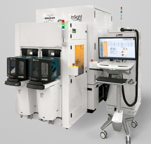
InSight AFP is the world’s highest performance and industry preferred CMP profiling and etch depth metrology system for advanced technology nodes. The combination of its modern tip scanner with inherently stable capacitive gauges and an accurate air-bearing positioning system enables non-destructive, direct measurements in the active area of dies.
InSight AFP's TrueSense® technology, with the proven long-scan capability of an atomic force profiler. Etch depth, dishing, and erosion on submicron features can be monitored fully automated with unsurpassed repeatability without relying on test keys or models. It’s unique
The Insight AFP combines the latest innovations in atomic force microscopy, including Bruker’s proprietary CDMode characterizing sidewall features and roughness. CDmode reduces the amount of required cross-sectioning, realizing significant cost savings. In addtion, AFP data provides a direct side-wall roughness measurement that cannot be obtained through other techniques.
The device killing defects of today's leading ICs are smaller than ever and require rapid resolution for HVM demands. The InSight AFP provides fast, actionable topographical and material information about defects on semiconductor wafers and phtomasks that allows manufacturers to rapidly identify sources of defectivity and eliminate their impact on production.
100x high-resolution registration optics and AFM Global Alignment enable less than ± 250 nm raw image placement accuracy for patterned wafer and mask ensuring that the defect of interest is the defect measured.
The system is fully compatible with KLARITY and most other YMS systems.
The Insight AFP combines the latest innovations in atomic force microscopy, including Bruker’s proprietary CDMode characterizing sidewall features and roughness. CDmode reduces the amount of required cross-sectioning, realizing significant cost savings. In addtion, AFP data provides a direct side-wall roughness measurement that cannot be obtained through other techniques.
Copyright © 2007 All Rights Reserved. 深圳市晧辰电子科技有限公司 版权所有 [粤ICP备14101712号-1] [法律顾问]
公司地址:广东省深圳市南山区西丽街道官龙村华纵科技楼5楼 邮编:518055