Product Description
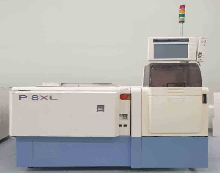
The TEL P-8XL is a fully automated wafer prober launched by Tokyo Electron Limited (TEL), specifically designed for the 200mm/300mm semiconductor wafer testing market. It supports high-precision, high-throughput automated testing requirements and is widely applied in the wafer-level electrical parameter verification of advanced chips such as high-performance CPUs and GPUs.
Key Features
High-Precision Alignment and Automatic Calibration: Utilizes industry-leading on Axis Alignment technology to precisely handle complex wafers with miniaturized terminal (PAD) sizes and narrow pitches, ensuring accurate contact between test probes and solder pads.
High-Throughput Design: Equipped with a high-speed Index (wafer transfer) system and a robust Stage (testing platform), it supports parallel testing across multiple sites, significantly improving Multi-measurement efficiency and reducing the testing cycle time per wafer.
Environmental Adaptability Testing Capabilities: Supports high- and low-temperature wafer measurements (e.g., extreme temperature testing from -65°C to +200°C), meeting stringent requirements for automotive-grade chips, AI chips, and other applications demanding environmental durability.
Compatibility and Scalability:
Wafer Size Compatibility: The P-8XL handles 200mm wafers, while the P-12XL extends to 300mm wafers, covering mainstream semiconductor manufacturing sizes.
Software Compatibility: Supports computer-based file management and remote operation (optional), enabling seamless integration into existing testing workflows and reducing deployment costs.
High-Voltage and Low-Interference Measurement: Optimized circuit design ensures low leakage and minimal noise interference during high-voltage testing, guaranteeing stable and accurate signal acquisition.